Data Sheet
28190
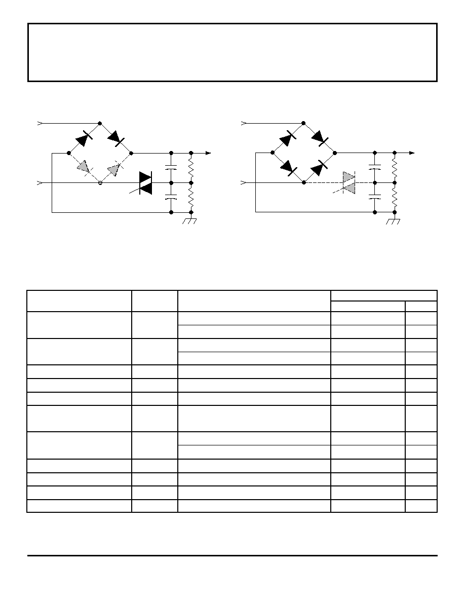
Intended for power supplies with universal inputs (85 V to 265 V
rms), the STR83145 and STR84145 latched, universal input-voltage
switches incorporate timing, control, and drive circuitry with a high-
current triac (bidirectional triode thyristor) switch. Each device senses
the applied ac line potential and automatically switches the rectifier and
associated capacitors between a voltage-doubler configuration (for line
voltages to 141 V) and a full-bridge configuration (for line voltages
greater than 149 V). This eliminates the possibility of user error with
adjustable jumpers or switches. Also, the related switch-mode power
stage need operate only over a reduced range of dc input voltages
when compared with "wide input" power supplies using a bridge rectifier
only. The reduction in dc input voltage range permits the use of lower-
voltage capacitors and leads to a reduction in power stage stresses and
power dissipation. The STR83145 and STR84145 differ only in their
maximum ac current rating (10 A and 12 A, respectively).
The internal sensitive-gate triac is switched by a temperature-
compensated constant-current gate driver driven by a 15 kHz pulse
train to reduce power dissipation. The switch-over voltage is accurately
set during manufacture for consistent operation. An user-adjustable
delay is provided to ensure start-up in the full-bridge mode. Once
established (by an input voltage greater than 149 V rms), an integral
latch holds the full-bridge mode to preclude false application of the
doubler mode during brownouts, voltage droops, or missing cycles.
The requirements of low transient thermal impedance and steady-
state thermal resistance are satisfied in a molded, 5-lead single in-line
power package. Similar input-voltage switches, with a switch point of
159 V rms, are also available.
FEATURES
s
Low Duty Cycle Triac Drive for Minimum Dissipation
s
For Universal Input Operation Between 85 V rms and 265 V rms
to 10 A or 12 A
s
Internal Latch Prevents False Mode Switching
s
Internal Sensitive-Gate Power Triac
s
Adjustable Start-Up Delay
s
Accurate 145 V rms Switch-Point Voltage
s
Low External Parts Count
s
Low Power Dissipation
s
Low-Power External Parts
Always order by complete part number:
Part Number
Max. On-State Current
STR83145
10 A rms
STR84145
12 A rms
LATCHED, UNIVERSAL
INPUT-VOLTAGE SWITCHES
ABSOLUTE MAXIMUM RATINGS
Repetitive Peak OFF-State Voltage,
V
DRM
............................................. 500 V
Static ON-State Current, I
T(RMS)
STR83145 ...................................... 10 A
STR84145 ...................................... 12 A
Non-Repetitive Surge ON-State Current, I
TSM
STR83145 .................................... 100 A
STR84145 .................................... 120 A
Package Power Dissipation,
P
D
........................................ See Graph
Triac Junction Temperature, T
J
..... +125
∞
C
Frame Temperature, T
M
................ +100
∞
C
Operating Temperature Range,
T
A
............................... -20
∞
C to +125
∞
C
Storage Temperature Range,
T
stg
............................. -40
∞
C to +125
∞
C
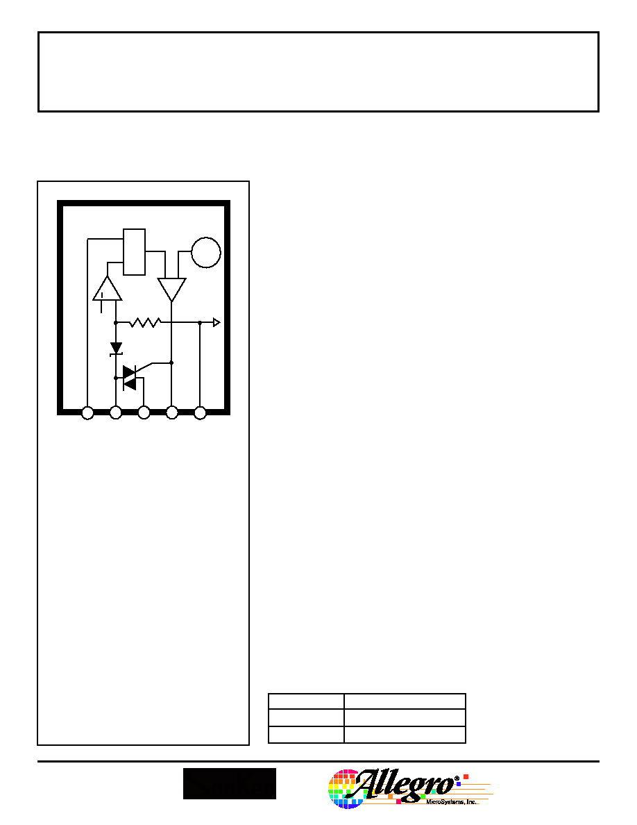
MT1
DELAY
COMMON
MT2
Dwg. PK-005
GATE
1
2
3
4
5
LATCH
+
OSC.
TM
STR83145
AND
STR84145
INTERIM ISSUE
(subject to change without notice)
August 16, 1994
STR83145
AND
STR84145
LATCHED, UNIVERSAL
INPUT-VOLTAGE SWITCHES
115 Northeast Cutoff, Box 15036
Worcester, Massachusetts 01615-0036 (508) 853-5000
TM
FUNCTIONAL BLOCK DIAGRAM
ALLOWABLE PACKAGE POWER DISSIPATION
COMMON
3
GATE
5
1
2
4
Dwg. FK-004
+
REG.
LATCH
+
+
DELAY
MT1
MT2
OSC.
7 V
30
20
10
20
60
100
40
FREE AIR
27 W
0
TEMPERATURE in
∞
C
ALLOWABLE PACKAGE POWER DISSIPATION in WATTS
INFINITE HEAT SINK
(NO MICA SHEET)
Dwg. GK-010
2 W
80
120
0
25
15
5
150 mm x 150 mm x 2 mm
(WITH MICA SHEET)
100 mm x 100 mm x 2 mm
(WITH MICA SHEET)
75 mm x 75 mm x 2 mm
(WITH MICA SHEET)
P IS LIMITED BY T
D
J
P IS LIMITED BY T
D
M
Copyright © 1994 Allegro MicroSystems, Inc.
SIMPLIFIED OPERATION
ELECTRICAL CHARACTERISTICS
at T
A
= +25
∞
C, voltage measurements are referenced to Common (pin 3)
(unless otherwise noted).
Limits
Characteristic
Symbol
Test Conditions
Min.
Typ. Max.
Units
On-State Voltage
V
TM
STR83145, I
T
= 10 A*
≠
≠
1.8
V
STR84145, I
T
= 12 A*
≠
1.6
≠
V
Off-State Current
I
DRM
STR83145, V
D
= 500 V
≠
≠
100
µ
A
STR84145, V
D
= 500 V
≠
40
≠
µ
A
Starting Voltage
V
S
V
T
= 2 V
≠
≠
100
V
Startup Time Delay
t
D
C
2
= 1
µ
F, V
MT1
100 V dc
40
≠
100
ms
DC Switch-Over Voltage
V
C
V
DELAY
1 V
200
205
210
V
Temperature Coefficient
of Switch-Over Voltage
VC
-20
∞
C
T
M
+100
∞
C
≠
±
45
≠
mV/
∞
C
Input Current
I
MT1
Voltage-doubler mode, V
MT1
= 195 V
≠
≠
10
mA
Full-bridge mode, V
MT1
= 400 V
≠
≠
6.5
mA
Delay Terminal Voltage
V
DELAY
≠
≠
7.0
V
Triac Gate-Drive Osc. Freq.
f
o
V
gate
ref. MT1, V
MT1
= 100 V
≠
15
≠
kHz
Latch Reset Voltage
V
R
V
GATE
= 400 mV
2.0
≠
15
V
Thermal Resistance
R
JM
FET channel to mounting surface
≠
≠
1.8
∞
C/W
NOTES: Negative current is defined as coming out of (sourcing) the specified device terminal.
Typical Data is for design information only.
*In practical use, I
T
is recommended derated to 70%.
+
+
85≠132 V rms
240≠373 V peak
+
+
174≠265 V rms
246≠373 V peak
Full-Bridge Mode
Dwg. EK-006
Voltage-Doubler Mode
STR83145
AND
STR84145
LATCHED, UNIVERSAL
INPUT-VOLTAGE SWITCHES
STR83145
AND
STR84145
LATCHED, UNIVERSAL
INPUT-VOLTAGE SWITCHES
115 Northeast Cutoff, Box 15036
Worcester, Massachusetts 01615-0036 (508) 853-5000
TM
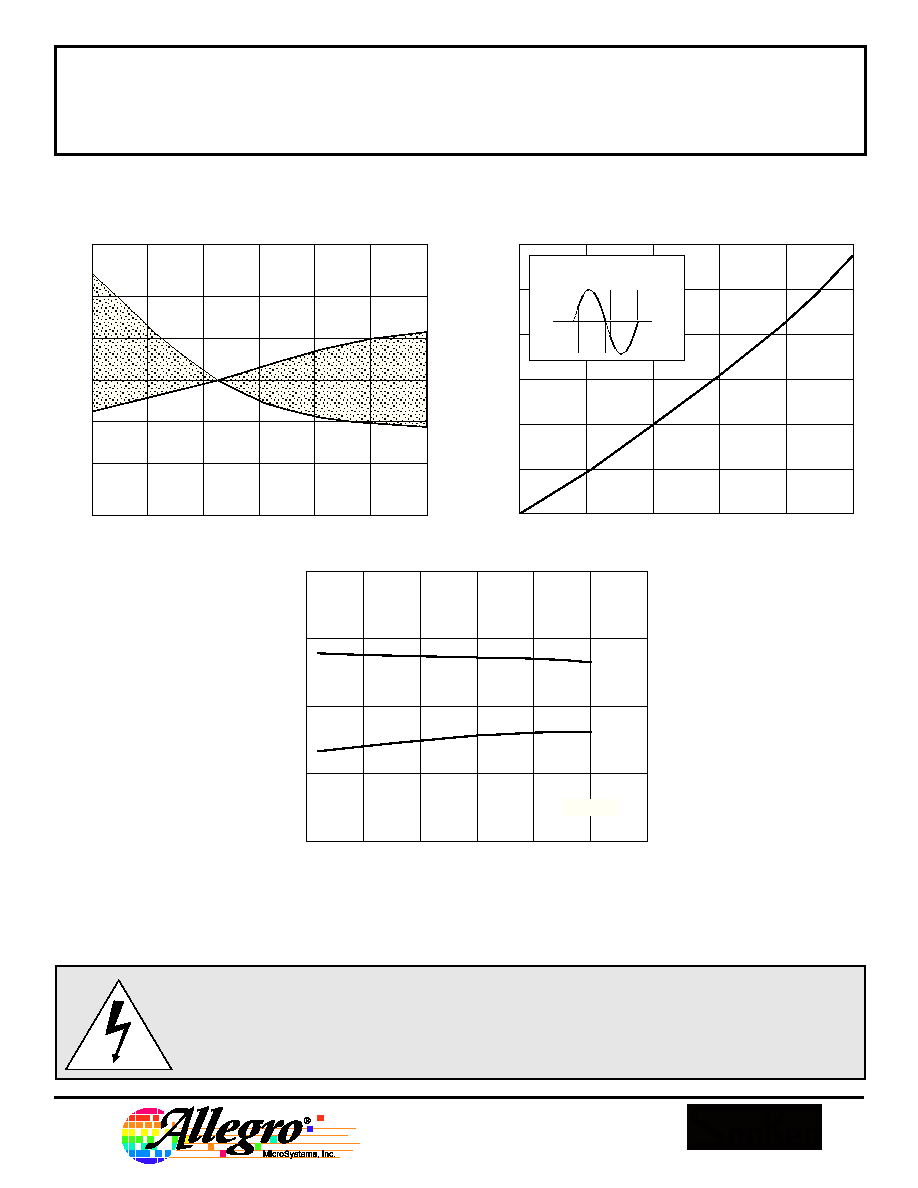
TYPICAL CHARACTERISTICS
APPLICATIONS INFORMATION
WARNING --
These devices are designed to be operated at lethal voltages and energy levels. Circuit
designs that embody these components must conform with applicable safety requirements. Precau-
tions must be taken to prevent accidental contact with power-line potentials. Do not connect
grounded test equipment.
The use of an isolation transformer is recommended during circuit development and breadboarding.
205
200
0
40
80
210
FRAME TEMPERATURE in
∞
C
DC SWITCH-OVER VOLTAGE in VOLTS
Dwg. GK-012
-20
20
60
100
4
2
0
2
6
STATIC ON-STATE CURRENT in AMPERES
AVERAGE ON-STATE POWER LOSS in WATTS
Dwg. GK-013
0
4
10
6
12
8
8
10
FULL SINE WAVE
CONDUCTION ANGLE
1 +
2
360
∞
1
2
40
20
-25
+50
+100
10
AMBIENT TEMPERATURE in
∞
C
TRIAC GATE-DRIVE DUTY CYCLE in %
Dwg. GK-008
30
0
0
+25
+75
+125
V
MT1
= 100 V
TRIAC GATE-DRIVE OSCILLATOR FREQUENCY in kHz
40
20
10
30
0
dc
F
O
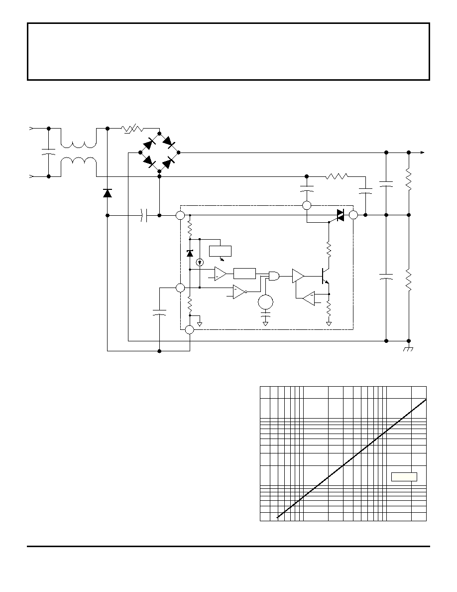
TYPICAL APPLICATION
300
100
30
1.0
10
C2 CAPACITANCE in
µ
F
VOLTAGE-DOUBLER MODE STARTUP TIME DELAY in ms
Dwg. GK-011
0.3
3.0
30
1000
3000
T = 25
∞
C
M
External component values have been selected for
optimum device performance and reliability. Except for
C
2
, component values other than the following may
result in false operation of these devices.
C
1
= 4.7
µ
F, 400 V
C
2
= 1
µ
F, 50 V
C
3
= 0.047
µ
F, 50 V
C
4
= 0.047
µ
F, 250 V
R
1
= 4.7
Turn-ON delay (forced full-bridge mode) may be
adjusted for desired system performance:
t
D
68 x C
2
where t
D
is the delay time in ms
C
2
is capacitance in
µ
F
+
+
+
3
5
1
2
4
Dwg. EK-007
+
+
+
+
R1
C4
C3
C1
C2
85≠265 V rms
240≠373 V peak
RM11C
RBV SERIES
-t
∞
STR83145
AND
STR84145
LATCHED, UNIVERSAL
INPUT-VOLTAGE SWITCHES